— ZELOCON / Technology

A superconducting platform, built on carbon.

1. ZELOCON’s material is re-ordered graphite with superconducting 2D interfaces.

2. Superconductivity lives in interface zones, not the bulk.

3. This makes it thin-film, lithographable and microelectronics-compatible.

The ZELOCON platform is a graphite-based superconducting system with a re-ordered crystal structure, engineered for room-temperature superconductivity for microelectronics.

— Operating principle

What is the ZELOCON material?

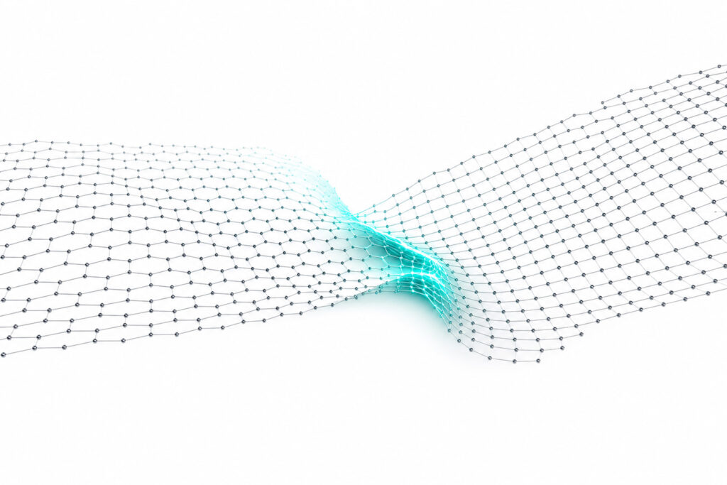
The ZELOCON material is a graphite-based system with a re-ordered crystal structure. The functionally decisive regions are two-dimensional interface zones within stacked graphite: transition regions between differently stacked domains — such as Bernal and rhombohedral regions — where a small relative twist between layers can further shape the electronic structure. Superconductivity is localized in these interfaces, not in the bulk.

— Four levers at once

Why does ZELOCON's approach matter?

ZELOCON’s approach matters because it pulls four levers at once: near-ambient operating temperature, abundant carbon instead of rare earths, design for integration, and intrinsically low noise. Together these target the total system cost of superconducting microelectronics, not a single specification.

01

Everyday operating temperature

A very high, near-ambient operating temperature (~300 K) could free entire device categories from the cryostat.

02

Carbon instead of rare earths

A material system based on widely available graphite simplifies supply chains and improves sustainability.

03

Built for integration

The prospect of translating superconducting principles into lithographable, microelectronics-compatible devices.

04

Low-noise by nature

Graphite’s extreme Debye temperature delivers an intrinsically favorable noise floor — the subject of a dedicated page.

— Technical profile

What are the key technical parameters of the ZELOCON material?

Parameters
Positioning
Classification

Operating temperature

Near room temperature (~300 K)

Company / technology figure

Material basis

graphite, re-ordered

Company / technology figure

Functional zone

2D interfaces (Bernal ↔ rhombohedral)

Company / technology figure

Debye temperature (in-plane)

≈ 2000–2300 K

Materials-physics reference value

Integration target

Thin-film, lithographable

Company / technology figure

Biocompatibility

100% (graphite)

Material property

Table 1 — Company / technology figures are labeled as such; the Debye temperature is a materials-physics reference value. Recommended schema: Dataset / PropertyValue.

— Operating principle

How is ZELOCON engineered at the interface, not the bulk?

ZELOCON is engineered at the interface because the superconducting effect is constructed in two-dimensional interface zones rather than doped into the bulk. This interface-first design is what lets the platform move toward thin-film and lithographable device geometries from the outset — the prerequisite for real microelectronics integration.

ZELOCON-specific values are treated as company / technology figures until comprehensive, independent device-level validation is publicly available. See the Validation page for the evidence path.

— Frequently asked questions

Frequently asked questions about the technology

Is ZELOCON's superconductivity in the bulk or at interfaces?

It is localized at two-dimensional interfaces within re-ordered graphite, not in the bulk — which is what enables thin-film, lithographable device geometries.

Is the material compatible with microelectronics manufacturing?

The platform is designed for thin-film, lithographable integration, with the goal of CMOS-adjacent, microelectronics-compatible fabrication. Device-level validation is ongoing.

Why the Debye temperature decides everything.

The critical temperature is only half the story. Graphite’s decisive advantage lies in thermal noise.